TFT-LCD displays have become the mainstream flat-panel display technology, gradually replacing traditional cathode-ray tube (CRT) displays. They are widely used in televisions, desktop monitors, laptops, car navigation systems, gaming consoles, PDAs, digital cameras, camcorders, and smartphones.
TFT-LCD technology originated in the late 1970s, initially using compound semiconductor materials like CdSe. However, the challenges in controlling the chemical composition during manufacturing led to the widespread adoption of silicon-based semiconductors in large-scale production, particularly in the TFT-LCD industry.
Most LCDs today use glass substrates, and due to limitations in processing temperatures, amorphous silicon (a-Si) and low-temperature polysilicon (LTPS) technologies are commonly employed for TFT fabrication. As the demand for TFT-LCDs increases, so does the requirement for improved display characteristics. To meet these demands, various display modes have been developed, including IPS (In-Plane Switching) and MVA/PVA (Multi-domain Vertical Alignment/Patterned Vertical Alignment).
However, due to the scope and practical application, this discussion focuses specifically on the TN (Twisted Nematic) mode, which is one of the most common display modes in TFT-LCD technology.
Structure of a TFT LCD Display (TN Type)
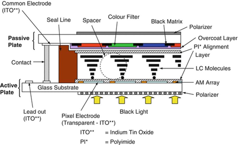
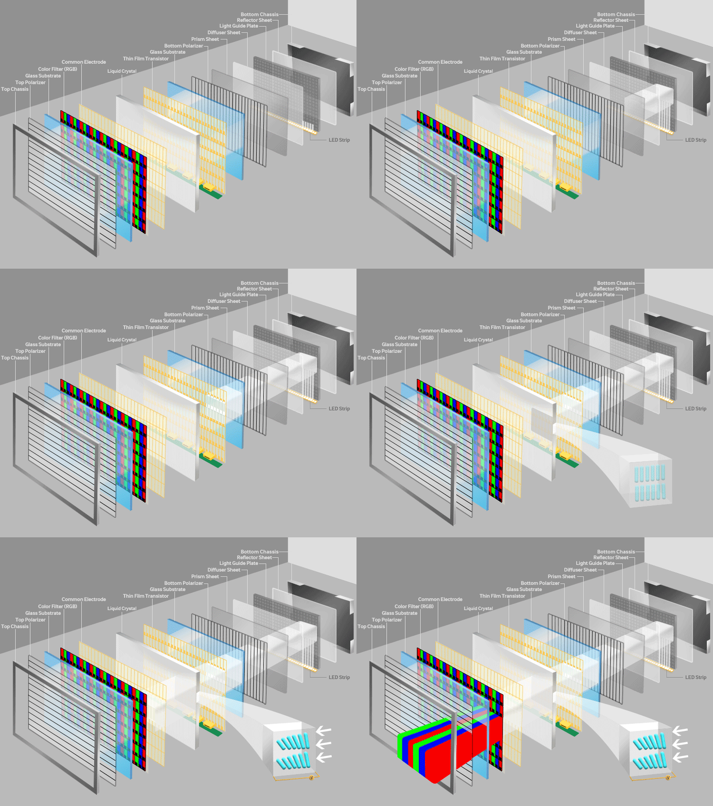
A TFT-LCD display module typically consists of several key components: the liquid crystal panel (Panel), the backlight unit, and external driving circuits. The liquid crystal panel itself is made up of two glass substrates sandwiching a layer of liquid crystals, along with polarizers placed on either side of the panel.
One of the glass substrates contains a color filter (CF) for color display, while the other substrate features an active matrix of thin-film transistors (TFT Array) for driving the pixels.
Let's Talk About How a TFT LCD Display Screen Is Made
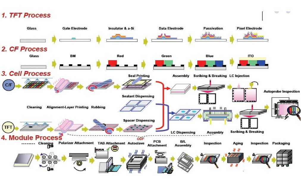
The production of a TFT (Thin Film Transistor) display panel can be divided into four main stages: TFT, CF (Color Filter), Cell, and Module. Each stage involves specific processes to create the final product.
1.Array Stage (TFT):
lBegins with the input of a white glass substrate.
l Ends with the completion of electrical circuit fabrication on the substrate.
2. Color Filter (CF) Stage:
lBegins with the input of a white glass substrate.
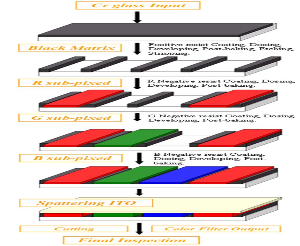
lEnds with the completion of the black matrix, RGB color filters, and ITO (Indium Tin Oxide) coating.
3.Cell Stage:
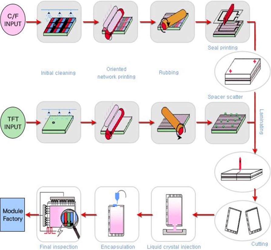
lInvolves aligning and bonding the TFT substrate with the CF substrate after orientation treatment.
lCompletes with cutting the bonded panels into individual units and attaching polarizer sheets.
4.Module Stage:
lStarts with the LCD panel.
lEnds with the assembly of the driving circuitry to form a complete display module.
Array Stage (TFT)
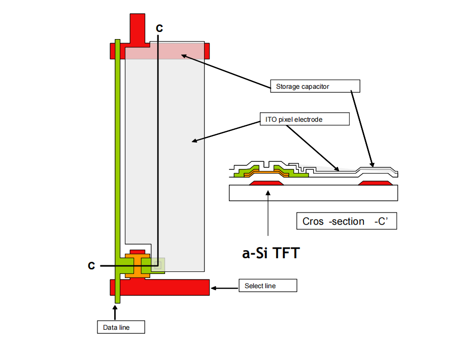
The array stage primarily completes the following steps: formation of the gate electrode and scan lines, deposition of the gate insulator and amorphous silicon islands, creation of the source and drain electrodes (S/D) along with the data electrodes and channel area, deposition of the protective insulation layer (passivation) and creation of via holes, and finally, the formation of transparent pixel electrodes (ITO).
Formation of the Gate and Scan Lines
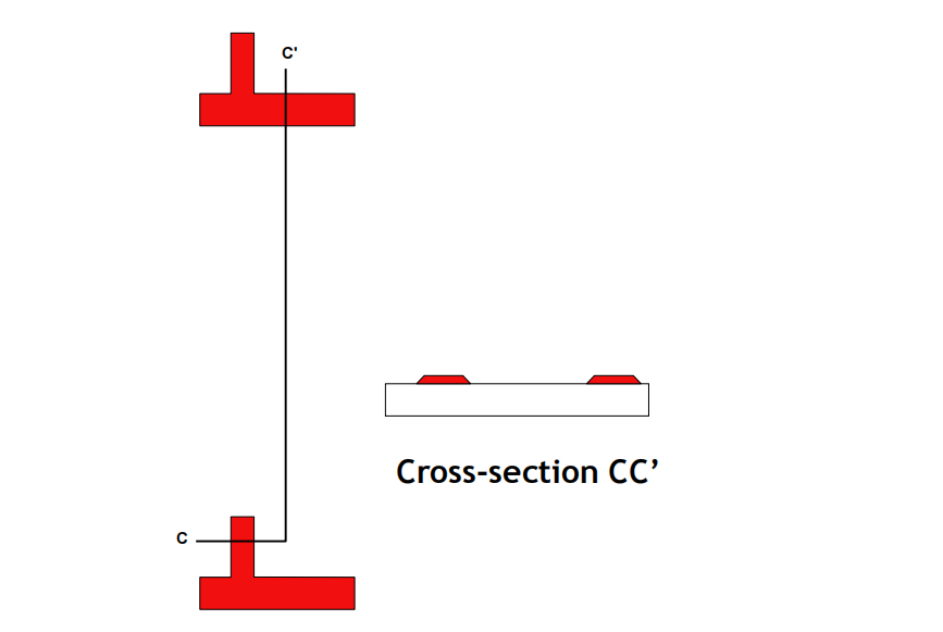
The process for forming the gate and scan lines begins with the initial and pre-coating cleaning of the glass substrate, followed by metal sputtering to deposit the gate material. Next, the substrate undergoes pre-coating cleaning, preparation for coating, and pre-bake. A photoresist layer is then applied, followed by post-coating bake, exposure through a mask, and development of the exposed photoresist. After post-develop bake, the substrate undergoes automated optical inspection (AOI) for defects, wet etching to remove unwanted material, stripping of the remaining photoresist, and post-strip cleaning. Finally, the substrate is inspected again using AOI to ensure quality. After completing these processes, the scan lines and gate electrodes are formed on the glass substrate.The resulting pattern is shown in the figure below.
Formation of the Gate Insulator and Amorphous Silicon Islands
The process for forming the gate insulator and amorphous silicon islands includes the following steps: pre-coating cleaning of the glass substrate, PECVD (Plasma-Enhanced Chemical Vapor Deposition) deposition of three layers for the gate insulator and amorphous silicon, pre-coating cleaning before photoresist application, pre-bake, photoresist coating, post-coating bake, exposure through a photomask, developing, post-develop bake, and automated optical inspection (AOI) for defect detection. Following this, the process continues with dry etching to remove unwanted material, stripping of the remaining photoresist, post-strip cleaning, and a final AOI inspection to ensure quality. Upon completion of these processes, the gate insulator and amorphous silicon islands are successfully formed on the glass substrate.
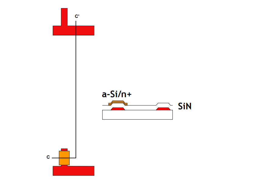
Formation of the Source and Drain Electrodes (S/D), Data Electrodes, and Channel
The process for forming the source and drain electrodes (S/D), data electrodes, and the channel includes the following steps: pre-coating cleaning of the glass substrate, metal sputtering to deposit the S/D layer, pre-coating cleaning before photoresist application, pre-bake, photoresist coating, post-coating bake, exposure through a photomask, developing, post-develop bake, and automated optical inspection (AOI) for defect detection. Following this, the process continues with wet etching to define the S/D electrodes, dry etching to form the channel, stripping of the remaining photoresist, post-strip cleaning, and a final AOI inspection to ensure quality. Upon completion of these processes, the source and drain electrodes, data electrodes, and the channel are successfully formed on the glass substrate, completing the TFT structure.
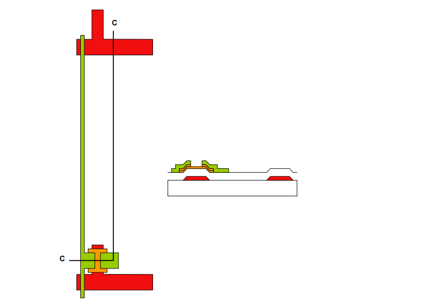
Formation of the Protective Insulation Layer (Passivation) and Vias
The process for forming the protective insulation layer (Passivation) and vias includes the following steps: pre-coating cleaning of the glass substrate, PECVD (Plasma-Enhanced Chemical Vapor Deposition) deposition of the passivation layer, pre-coating cleaning before photoresist application, pre-bake, photoresist coating, post-coating bake, exposure through a photomask, developing, post-develop bake, and automated optical inspection (AOI) for defect detection. Following this, the process continues with dry etching to form the vias, stripping of the remaining photoresist, post-strip cleaning, and a final AOI inspection to ensure quality. Upon completion of these processes, the protective insulation layer and vias are successfully formed on the glass substrate, completing the TFT structure.
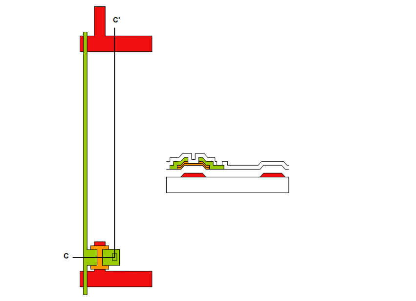
Formation of the Transparent Pixel Electrodes (ITO)
The process for forming the transparent pixel electrodes (ITO) includes the following steps: pre-coating cleaning of the glass substrate, sputtering deposition of the ITO layer, pre-coating cleaning before photoresist application, pre-bake, photoresist coating, post-coating bake, exposure through a photomask, developing, post-develop bake, and automated optical inspection (AOI) for defect detection. Following this, the process continues with wet etching to define the ITO electrodes, stripping of the remaining photoresist, post-strip cleaning, and a final AOI inspection to ensure quality. Upon completion of these processes, the transparent pixel electrodes are successfully formed on the glass substrate, completing the array fabrication process.
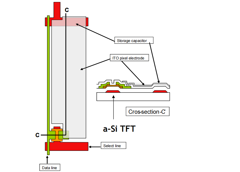
Color Filter (CF) Stage
The Color Filter (CF) is a critical component of TFT-LCD (Thin-Film Transistor Liquid Crystal Display) panels, essential for generating vibrant color images. It consists of a sequence of red, green, and blue pixels that combine to produce a full spectrum of colors on the display. Below is a detailed overview of the structure and fabrication process of a Color Filter:Structure of a Color Filter
A Color Filter typically consists of multiple layers, each serving a distinct function:
1.Glass Substrate:
The foundational base layer that provides mechanical support.
2.Black Matrix (BM):
Constituted of a light-absorbing material, it delineates each pixel and minimizes inter-pixel light leakage, improving contrast.
3.Color Resin Layers:
The actual red, green, and blue-colored filters that determine the pixel colors, crafted from a dyed transparent resin material.
4.Overcoat Layer (OC):
A protective layer overlaid on the color resins to even out the surface and shield the filters from physical and chemical harm.
5.ITO (Indium Tin Oxide) Electrode:
A transparent conductive layer that enables the panel to operate as an electrode, regulating the light that passes through.

Manufacturing Process of a Color Filter
lCreating a Color Filter involves several precise steps, often utilizing photolithography techniques similar to those used in semiconductor manufacturing:
1.Substrate Preparation:
lThorough cleansing of the glass substrate to eradicate impurities that could compromise CF quality.
2.Black Matrix Formation:
lApplying a photoresist layer to the cleaned substrate, photolithography is utilized to outline the BM pattern. Post-exposure, undeveloped areas are revealed and filled with black pigment, then cured.
3.Color Resin Application:
lSuccessive application of red, green, and blue color resins within the BM confines using a distinct photolithography process for each color layer. After coating and exposure, the areas without photoresist are developed and filled with the resin, followed by curing.
4.Overcoat Layer Application:
lAn OC layer is applied atop the resin colors to protect them and establish a smooth surface for subsequent ITO electrode deposition.
5.ITO Electrode Deposition:
lThe transparent ITO electrode is sputter-deposited onto the OC layer, then patterned to structure the electrode architecture.
6.Inspection and Testing:
lMeticulous inspections and tests throughout production ensure CF quality. Metrics like color fidelity, uniformity, and defect levels are thoroughly examined.
7.Integration:
lPost-quality assurance, the Color Filter is precisely aligned and laminated with TFT-LCD panel constituents such as the TFT array and the liquid crystal layer.
The fabrication of the Color Filter reflects a delicate interplay between chemical engineering and precision photolithography, crucial for the vibrant color display evident in TFT-LCD screens.
Cell Stage
The production process within the 'Cell' aspect of a TFT display can be divided into four key stages: Alignment, Boxing, Cutting, and Polarizer Attachment. The objectives and primary procedures of these stages are summarized as follows:
PI (Polyimide) Printing
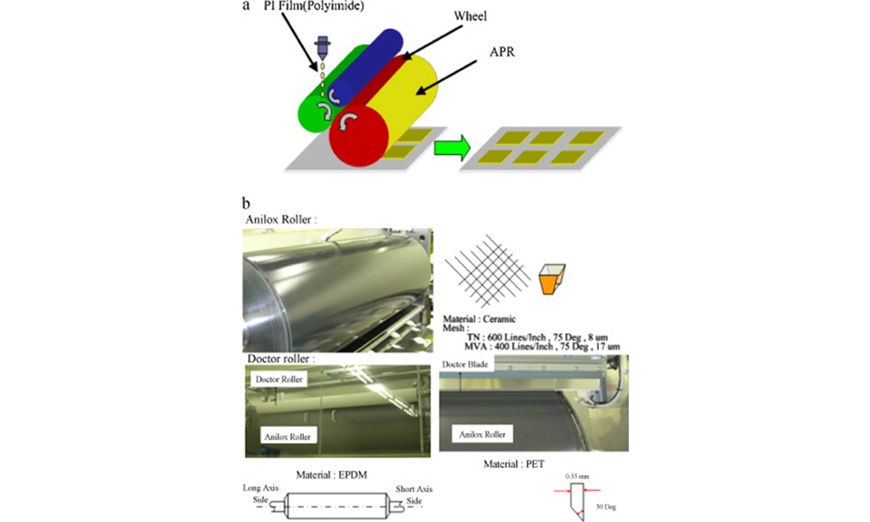
Polyimide (PI) is a high-performance, transparent organic polymer material that, after application and baking, firmly adheres to the surfaces of the CF and TFT substrates. The coating of PI utilizes a specialized gravure printing technique. Besides the primary gravure printing process, PI printing involves several auxiliary processes, including substrate cleaning, pre-baking, automatic optical inspection, and curing. If necessary, there is also a PI rework process.
1.Pre-PI Cleaning:
Thoroughly clean the substrate to ensure it is free from dust, grease, and other contaminants, preparing it for the next steps.
2.PI Printing:
Apply the PI (Polyimide) material onto the substrate, similar to printing a design on paper, but using a special material that forms a protective layer.
3.Pre-Baking:
A preliminary baking phase that partially dries the PI layer to ensure proper adhesion to the substrate.
4.PI Inspection:
Close examination of the printed layers for any smudges, uneven areas, or defects, similar to inspecting a painted wall for imperfections.
5.PI Rework:
If any issues are identified during inspection, this step involves correcting those imperfections, akin to erasing mistakes on a sketch.
6.PI Curing:
The PI layer is fully hardened through a baking process, rendering it strong and durable, much like clay is hardened in a kiln.
Rubbing Process
The friction process consists of three primary stages: Ultrasonic Cleaning (USC), Alignment, and Rubbing, with an additional post-rubbing USC cleaning step. Here's a detailed breakdown:
1. Ultrasonic Cleaning (USC):
- Aimed at removing dust and particles from the substrate using an ultrasonic cleaner, which employs ultrasonic waves for thorough cleaning. This ensures the substrate is free from any contaminants before proceeding to the next steps.
2. Alignment:
- The alignment phase adjusts the substrate's orientation to fulfill visual requirements. This process is straightforward, focusing on positioning the substrate correctly for subsequent treatments.
3. Rubbing:
- During the rubbing stage, a velvet cloth is used to rub over the PI layer. This action aligns the PI's side chains in a unified direction, organizing the molecular structure to achieve the desired surface properties.
4. Post-Rubbing Ultrasonic Cleaning (USC):
- After rubbing, the substrate may have particulate matter or residues. The post-rubbing USC cleaning removes these residues, ensuring the substrate's surface is impeccably clean. This step is critical for maintaining the quality of the final product, as it uses ultrasonic waves to dislodge and remove any particles or residues adhered during the rubbing process.

ODF (One Drop Fill) Encapsulation Process
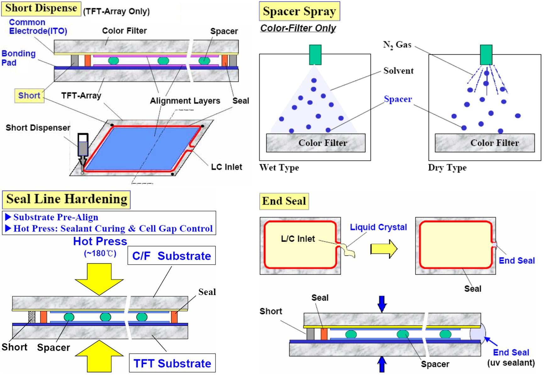
In the manufacturing process of TFT-LCD, the "cell assembly process" is a critical step that involves tightly bonding the color filter (CF) and TFT glass substrate together, filling the gap (commonly referred to as the "cell") between the two glass substrates with liquid crystal, and precisely controlling the thickness of the cell. The traditional cell assembly method involves creating an empty cell first, then injecting the liquid crystal. In contrast, the One Drop Fill (ODF) technology involves initially dropping liquid crystal on the TFT or CF glass substrate, then bonding the two substrates together in a vacuum environment, and completing the cell assembly using ultraviolet (UV) light and thermal curing techniques.
The ODF cell assembly process is primarily divided into five major steps:
1. Sealant and Silver Paste Application:
- UV-curable adhesive is used as the sealant, applied along the edges of the CF and TFT glass substrates, to ensure that the two substrates are firmly bonded and to define the thickness of the cell. Simultaneously, the application of silver paste is for connecting the common electrodes on CF and TFT to ensure electrical connectivity.
2. Liquid Crystal Coating:
- Liquid crystal material is dropped onto the TFT substrate that has already been coated with the sealant. The liquid crystal material plays a critical role in the display process; it adjusts the state of light passing through by changing its arrangement, thereby controlling the color and brightness of pixels.
3. Vacuum Bonding:
- The CF substrate, which has been coated with the sealant, silver paste, and liquid crystal, is bonded with the TFT substrate in a vacuum environment. This step helps prevent the formation of bubbles and ensures that there is a tight, gapless bond between the two substrates.
4. Ultraviolet (UV) Curing:
- To prevent damage to the liquid crystal, a light-shielding film is used to cover sensitive areas, followed by exposure of the bonded substrates to ultraviolet light. This process enables the sealant and silver paste to cure quickly and form a strong bond.
5. Thermal Curing:
- After the UV curing is complete, the substrates undergo a thermal process to further strengthen the adhesion of the sealant. This step is particularly aimed at areas not fully reached by UV light, such as under the leads, ensuring that these parts are thoroughly cured.
Furthermore, in addition to these four main process flows, ODF cell assembly also includes some auxiliary processes, such as cleaning before pad material application, reworking of pad material, USC dry cleaning before sealant and liquid crystal application, automatic optical inspection after sealant application, and visual inspection, as well as cell thickness and offset detection after the sealant has cured. Although these steps are auxiliary, they play a crucial role in ensuring the rigor of the entire production process and the quality of the final product.
Cutting, Edging, and Electrical Measurement Process
1. Cutting:
- Due to the definite size of the glass substrate and the variety in product sizes, multiple product cells are arranged on a single glass substrate. Cutting is performed by sliding a diamond wheel across the glass surface. With advancements in cutting wheel technology, a technique now creates a very deep cut mark, eliminating the need for debonding.
2. Edging:
- After the glass is cut into individual screens, each screen's edges have many fine cracks. To prevent these cracks from causing breakage due to collisions in subsequent handling, edging treatment is necessary.
3. Electrical Measurement:
- Electrical measurement is an auxiliary process used multiple times during production, but it is especially crucial here as this is the first time electricity is applied to test the LCD's display performance. The testing principle is simple: apply electricity to individual display pixels and observe the cell's display performance through a polarizing film. Typically, a short bar used for array testing is electrified. After electrical testing, screens that do not meet standards are removed to prevent waste of materials in later stages.
Additionally, auxiliary processes include post-cutting visual inspection and post-edging cleaning, which are crucial for ensuring the rigor of the entire production process and the quality of the final product.
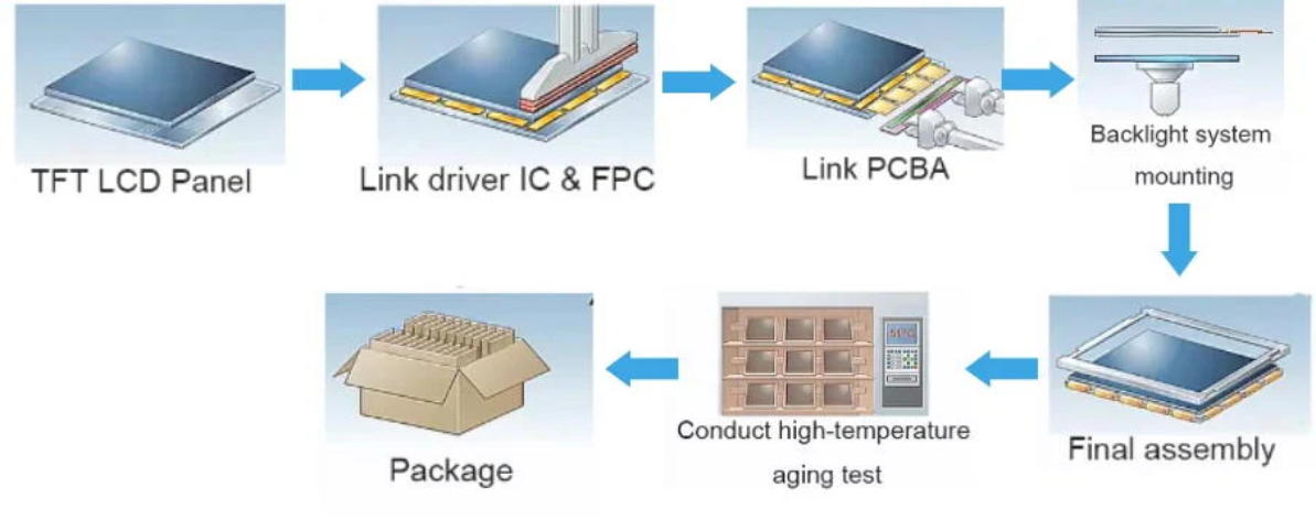
TFT Display Module Assembly Process
The assembly of TFT (Thin Film Transistor) display modules involves several key steps:
1. COG & FPC Bonding
- COG (Chip On Glass) and FPC (Flexible Printed Circuit)bonding are methods for connecting circuits.
- Process: An electrode array is formed on the glass substrate, which is then aligned with a corresponding array on the IC/FPC. Anisotropic Conductive Film (ACF) is used to connect each IC/FPC electrode with the glass electrode.
2. Applying the Polarizing Film
- Purpose: Since LCD operation relies on polarized light, attaching a polarizing film is crucial. This film controls the light passing through the liquid crystal cells to create images.
3. Assembly
- Components: The backlight, screen, control circuit board, and other elements such as touchscreens are brought together to form a complete display module.
- Procedure: This step is typically performed manually by skilled technicians who ensure the quality of the assembled modules.
These processes are fundamental to the production of high-quality TFT display modules.
Auxiliary Processes in TFT Display Module Assembly
In addition to the main processes, the module segment includes several auxiliary processes to ensure the functionality and reliability of TFT display modules:
1. Laser Cutting and Post-Cutting Electrical Measurement
- Components are precisely cut using a laser, followed by electrical testing to ensure they meet the required specifications.
2. Bonding and Post-Bonding Electrical Measurement
- Electrical testing is performed after the COG and FPC bonding processes to verify the integrity of these connections.
3. Microscopic Inspection
- Microscopic inspections (or Automated Optical Inspection (AOI) for FPC bonding) are conducted after laser cutting and bonding to check for any defects or issues.
4. Peel Strength Test
- Peel strength tests are done after IC bonding and FPC bonding to evaluate the durability of the bonds.
5. Aging After Assembly
- The assembled modules undergo an aging process with power applied to ensure long-term reliability.
6. Packaging and Shipment
- Once the modules pass all tests and inspections, they are packaged and shipped to the customer or the next phase of production.
These stages collectively ensure the functionality and reliability of TFT display modules, from individual component assembly to the final checks before the modules are ready for distribution.
TN Display Mode Advantages
Fast Response Time: TN displays offer fast response times, typically ranging from 1 to 5 milliseconds, making them suitable for displaying rapidly changing images such as games and videos.
1. Low Cost: Due to mature production processes, TN displays have lower manufacturing costs, making them ideal for mass production and budget-friendly options.
2. Low Power Consumption: TN displays consume relatively low power, contributing to longer battery life in portable devices like laptops and tablets.
3. Wide Availability: TN technology is widely adopted, making it easy to find replacement parts and support.
4. Simple Manufacturing: The simplicity of TN technology means that it is easier to manufacture compared to more advanced display technologies, which translates into cost savings for consumers.
5. Bright and Clear Text: TN displays are known for their clear and bright text, making them well-suited for office and document-centric applications.
6. Reliability: TN displays are generally reliable and have a long lifespan, which is beneficial for businesses and individuals looking for durable displays.
These advantages make TN displays a popular choice for a wide range of applications, from budget monitors to laptops and other portable devices.
TN Display Mode Disadvantages
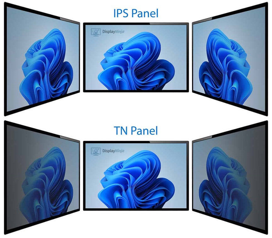
1. Narrow Viewing Angle: TN displays have a narrow viewing angle, typically around 160 degrees. When viewed from the side, the image quality significantly decreases, affecting the overall viewing experience.
2. Limited Color Reproduction: TN displays have limited color reproduction capabilities, resulting in less vibrant and less accurate colors compared to more advanced display technologies.
3. Lower Contrast Ratio: TN displays typically have a lower contrast ratio, meaning blacks appear less deep and whites are less bright, leading to less vivid image quality.
4. Image Shift: Due to the narrow viewing angles, TN displays may exhibit color shifting or inversion when viewed from different angles, which can be distracting.
5. Limited Grayscale Performance: TN displays often struggle with grayscale performance, which can affect the quality of monochrome images and text.
6. Limited HDR Support: High Dynamic Range (HDR) content is not well-supported on TN displays, limiting the display's ability to show the full range of brightness and color detail present in HDR content.
7. Limited Customization Options: TN displays often lack advanced settings and customization options available on higher-end display technologies, which can limit user control over image quality.
These disadvantages can impact the overall viewing experience, particularly for users who require high-quality visuals, such as graphic designers, photographers, and gamers.
Applications of TN Display Mode
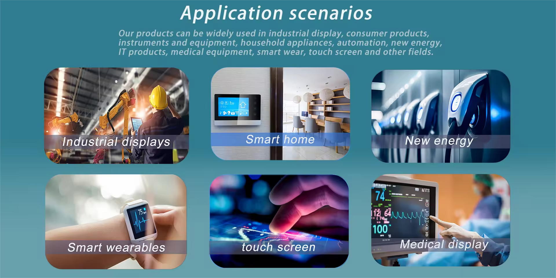
1. Consumer Electronics: Due to their low cost and fast response times, TN displays are widely used in consumer electronics such as laptops, desktop monitors, and gaming displays.
2. Industrial Equipment: In industrial control systems, TN displays are preferred for their quick response and low power consumption, making them suitable for real-time monitoring and control applications.
3. Medical Devices: Portable medical devices often incorporate TN displays for their fast data readout and display capabilities, enabling efficient patient monitoring and diagnostics.
4. Point-of-Sale (POS) Systems: TN displays are commonly found in POS systems, where their reliability and cost-effectiveness are advantageous.
5. Educational Tools: In educational settings, TN displays are used in interactive whiteboards and student devices, providing a cost-effective solution for learning tools.
6. Transportation Systems: TN displays are utilized in transportation applications, such as vehicle dashboards and navigation systems, where their low power consumption and durability are beneficial.
These applications leverage the strengths of TN displays, making them a versatile and practical choice in various industries.
Latest articles
-
Can TFT displays operate in extreme temperatures?
Yes, TFT displays can operate in a wide range of temperatures, typically from -20°C to 70°C, with so
-
Are TFT displays resistant to dust and water?
TFT displays themselves are not inherently resistant to dust and water. However, they can be housed
-
What is the typical contrast ratio for a TFT display?
The typical contrast ratio for a TFT display ranges from 500:1 to 1000:1, offering good visibility i
-
What is the typical viewing angle for a TFT display?
The typical viewing angle for a TFT display is around 160° horizontally and 160° vertically, providi
-
What is the refresh rate of a TFT display and why is it important?
The refresh rate of a TFT display is typically 60Hz. A higher refresh rate can reduce motion blur an


